Microelectronics technology product design began transitioning from mature hybrid microcircuit technology to Multi-Chip Modules (MCMs) in the early 1990s to meet the increasing performance demands and the trend of compact for portable consumer electronic products in the market.
Today, heterogeneous integration of chips is prominent, leading to mass production of advanced semiconductor packaging technologies to reduce power consumption, shrink size, and improve performance. This has also sparked higher discussions on Known Good Die (KGD) solutions. In this article, let's explore what KGD Die means and why it plays a crucial role in the inevitable trend of semiconductor development.
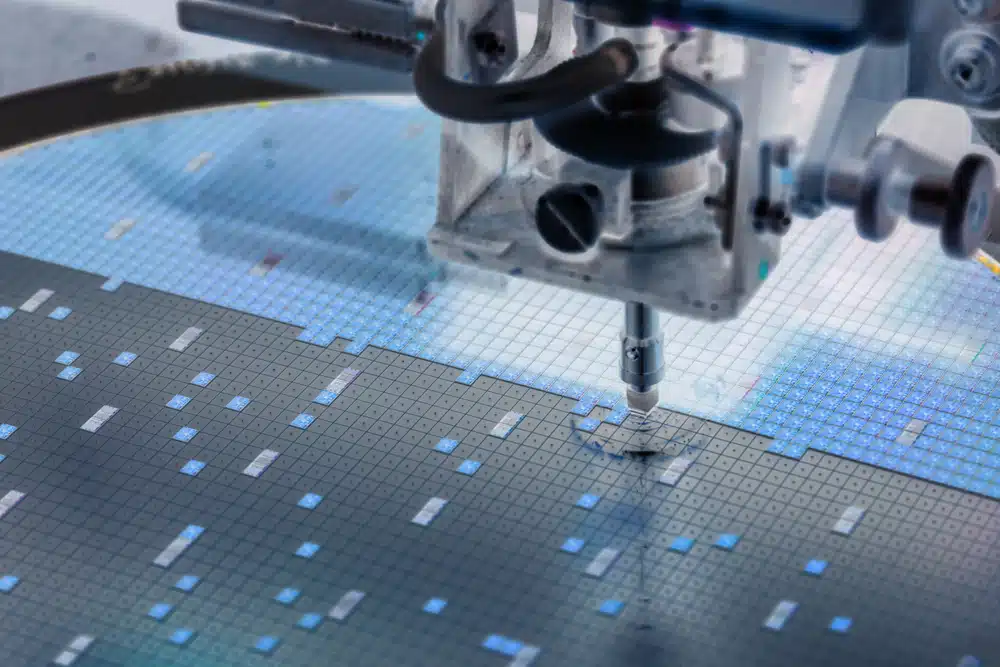
Literal Explanation - Known Good "Die": KGD stands for "Known Good Die." Before delving into its definition and application, let's understand the differences among a wafer, die, and chip:
What is a Known Good Die (KGD/KGD Die)?
KGD is translated as "良品裸晶粒" in Chinese and is interchangeably used with terms like KGD Dram and KGD Die in the industry.
The complete definition of KGD: A bare die or unpackaged chip that has undergone extensive testing and is confirmed to possess the same quality, reliability, and functionality as the packaged product, meeting specified functional and specification standards. Semiconductor manufacturers use KGD dies, packages them into a single chip with their own products, conducts final tests, and ships them to end-users.
KGD differs from regular packaged transistors as it is an unpackaged die. This feature allows it to be used in System-in-Package (SiP) and Multi-Chip Package (MCP) configurations, facilitating heterogeneous integration. This means stacking chips in 3D or configuring them in 2.5D to integrate different electronic components such as logic chips, memory, and radiofrequency elements in the same package, achieving high performance, low power consumption, and compact designs on a system level.
Interpreting the Industrial Applications of KGD:
The Area Array Interconnection Handbook compares how KGD applications affect different levels of MCM packaging and summarizes two principles:
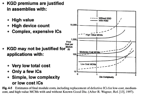
Source: Bertin, Claude & Su, Lo-Soun & Horn, Jody. (2001). Known Good Die (KGD). 10.1007/978-1-4615-1389-6_4.
In the wave of digital transformation, emerging technologies such as the Internet of Things (IoT), big data, and AI are commercializing, driving a new growth phase in the semiconductor industry. The demand for innovative chip products is stronger than ever. However, it is undeniable that the traditional Moore's Law's 2D process scaling is slowing down.
Shifting from mere size scaling to "More than Moore," which integrates different types of chips, and the demand for advanced wafer processes and packaging technologies have triggered more diverse KGD product applications. These applications go beyond traditional mobile devices, consumer electronics, digital video conversion boxes, digital cameras, and wearable technologies, extending into promising fields like satellite positioning, 5G communication, smart factories, and automotive electronics.
Why is KGD widely adopted? Observing the Trend of KGD and Chip Testing:
Facing the next decade of the semiconductor industry, new challenges arise in chip development regarding precision and speed. Moving from 2D to 3D integration with high chip integration capabilities has become a key factor in product differentiation. KGD can serve as the stepping stone for the IC industry's PPACt (Power, Performance, Area, Cost, and Time-to-Market) technology roadmap. Through chip-level and system-level improvements and innovations, long-term profitability and growth capabilities can be enhanced.
There are various KGD solutions in the market to meet different application needs. Among them, "Application-Oriented Buffer Memory KGD" is adopted by 4C consumer electronics companies. It not only fulfills performance requirements but also offers several product advantages:
Different from System-on-Chip (SoC), which integrates multiple functionalities such as processors and memory into a single chip, "Application-Oriented Buffer Memory KGD" achieves heterogeneous vertical integration through 2.5D/3D stacking of different types of logic, memory, analog, radiofrequency, and flash memory dies. This results in high flexibility, integration, and broad application prospects, significantly boosting the performance of electronic products.
KGD is the preferred choice for chip suppliers when providing system-level packaging (SiP) to customers, simplifying system design, and reducing chip size. Since 2000, Etron Technology has been engaged in the mass production of KGD memory and has received various honors, including the Intel Supplier Award. To date, over 2.6 billion KGD dies have been shipped. Etron Technology’s application-oriented buffer memory KGD adopts innovative circuit design and undergoes rigorous wafer-level aging testing. While ensuring product quality, it also meets cost-effectiveness. With its small size and high integration capability, it effectively enhances the performance of electronic products. Additionally, it provides customized services to assist in using high-quality chip raw materials, reducing costs, and aligning with current trends, making it highly favored by consumers and cooperation partners.