
The RPC DRAM is a new DRAM architecture that may be unfamiliar but as will be shown, offers the best overall SWaP-C for endpoint video processing nodes.
In the first part of this two-part article, we noted that processing is getting pushed toward the edge and into endpoints. We demonstrated that there may be an opportunity to reduce overall size, weight and power / cost (“SWaP-C”) by adopting a distributed architecture using localized endpoint-based processing versus using a COTS (commercial off the shelf) edge processor optimized for media processing. Parts that have a lot of overhead can be cheap up front, but can end up using more overall power, occupy more XYZ space at higher weight and may have concentrated thermal dissipation concerns.
Performing a SWaP-C analysis will reveal if that will be the case or not. One of the components most likely to be overprovisioned is memory, and we will show how that can aggravate SWap-C in several ways. In this second installment, we’ll discuss a new version of DRAM that addresses the issue.
RPC DRAM
The RPC DRAM is a 256 Mbit device and has a x16 data bus that operates with DDR-type signaling. The clock speed can operate up to 1200 MHz (“DDR2400”) leading to a single device bandwidth of up to 4800 Megabytes/sec.
The device has a four-bank organization and is capable of overlapped row and column operations like standard DDR/LPDDR type DRAM.
The RPC DRAM has a 24-switching signal interface when using byte-wide data strobes or a 22-pin interface if the optional 16-bit data strobe mode is used.
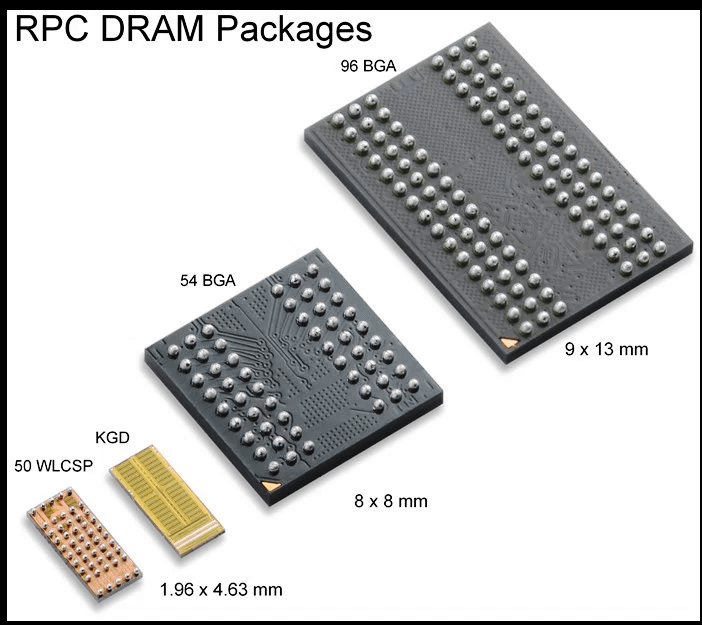
RPC DRAM packages
Packaging
The packaging choices for the RPC DRAM are shown in Figure 4. On the right is a standard 96 ball 9 x 13 mm BGA as would be used for a x16 DDR3/4 device. The RPC DRAM in that package is interchangeable with DDR3 in certain systems (more on that below). On the far left is the 50 ball 1.96 x 2.63 mm wafer level CSP (WLCSP), the first DRAM in the world to be offered in such a package. Next to it is the Known Good Die (“KGD”) bare die version that is typically used in stacked die multichip packages (MCPs). Note the bonding pads along the bottom edge. The small BGA next to it is the 54 ball 8 x 8 mm BGA. It combines a reduced package size vs DDR3/4 in a 0.8 mm ball pitch packaging technology for low cost PCB fabrication.
The power advantage of RPC
For power, the RPC DRAM uses the least operating current versus other memory subsystem implementations of similar bandwidth using x16 DDR3/4, or x16 / x32 LPDDR3/2.
Unfortunately, these DDR/LPDDR type devices generally are not obtainable in capacities lower than 1 gigabit and some, like DDR4, are offered in 4 Gbit as the smallest capacity. Consequently, a DDR3, LPDDR3 or DDR4 solution selected solely on the basis of bandwidth generally means energizing far more bits than needed for the job which burns unnecessary power.
For example, a baseline frame buffer design for 4K60 video typically requires about 200 megabits and needs the bandwidth of a x16 bus operating between DDR667 and DDR1600. Typically, 1, 2, or 4 Gbit DDR/LPDDR-type devices are used: up to now, that’s been the best of the alternatives, even though it is wasteful of energy and silicon area.
In contrast, the RPC DRAM’s capacity and bandwidth are ideal for video buffering applications: it is 256 Mbit capacity and its x16 DDR-type interface operates as high as DDR2400 (MT/s). Using the WLCSP, the PCB footprint is smaller than for a larger capacity device, and the current is the least of the alternatives.
Using the RPC DRAM for video buffering means there are fewer wasted bits in the frame buffer RAMs that consume power and fewer signals switching during active data transfer. Both result in significant power savings as shown in the graphs below.
Memory subsystem comparison: current consumption graphs
The memory choices for a 4K/60 node are considered on the basis of bit count and bandwidth. For a 16-bit color depth approximately 133 megabits are required and to fully write two and read one entire video frame during the time of an incoming video frame (like accessing 180 f/s) requires a 16-bit channel running at DDR1550 MT/s approx.
Some FPGAs are incapable of operating DDR3 type memory at full clock speed. As a result, data paths approximately twice as wide as needed for full speed operation must be used. For that reason, both 16-bit and 32-bit wide implementations are examined.
The JEDEC Standard memory ICs considered were:
1 Gbit x16 DDR3, 1 Gbit x32 LPDDR3, 1 Gbit x16 LPDDR3, 2 Gbit x32 LPDDR2, 4 Gbit x32 LPDDR3, 4 Gbit x16 DDR4 and 8 Gbit x16 DDR4.
Some of these JEDEC standard devices are early in their manufacturing life while some are near the end. The non-standard devices considered were 256 Mbit x16 RPC DRAM and 64 Mbit x8 HyperRAM™.
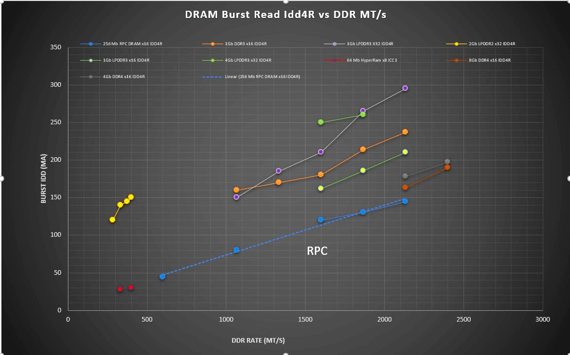
DRAM burst read current vs DRAM pin speed (click on the image for larger view).
In Figure 5 is a graph that compares single memory devices on the basis of their operating current during burst read operations. The smaller number of switching IOs combined with the smaller number of energized bits means the RPC DRAM uses the least amount of current for a given clock speed. To see a more complete picture, it is useful to look at the single device bandwidth, as shown in the graph below.
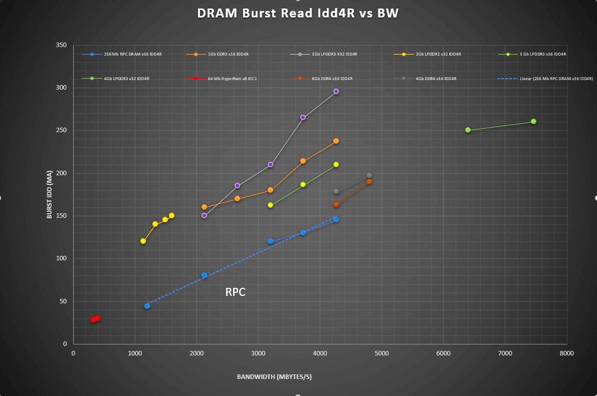
DRAM burst read current vs single DRAM bandwidth (click on the image for larger view).
The graph in Figure 6 compares the same devices but plots the burst operating current against single device bandwidth. That captures the impact of the device’s bus width on the system bandwidth to allow devices of x8, 16 and x32 organization to be compared on the same basis when evaluating candidates for memory used in bandwidth-hungry applications.
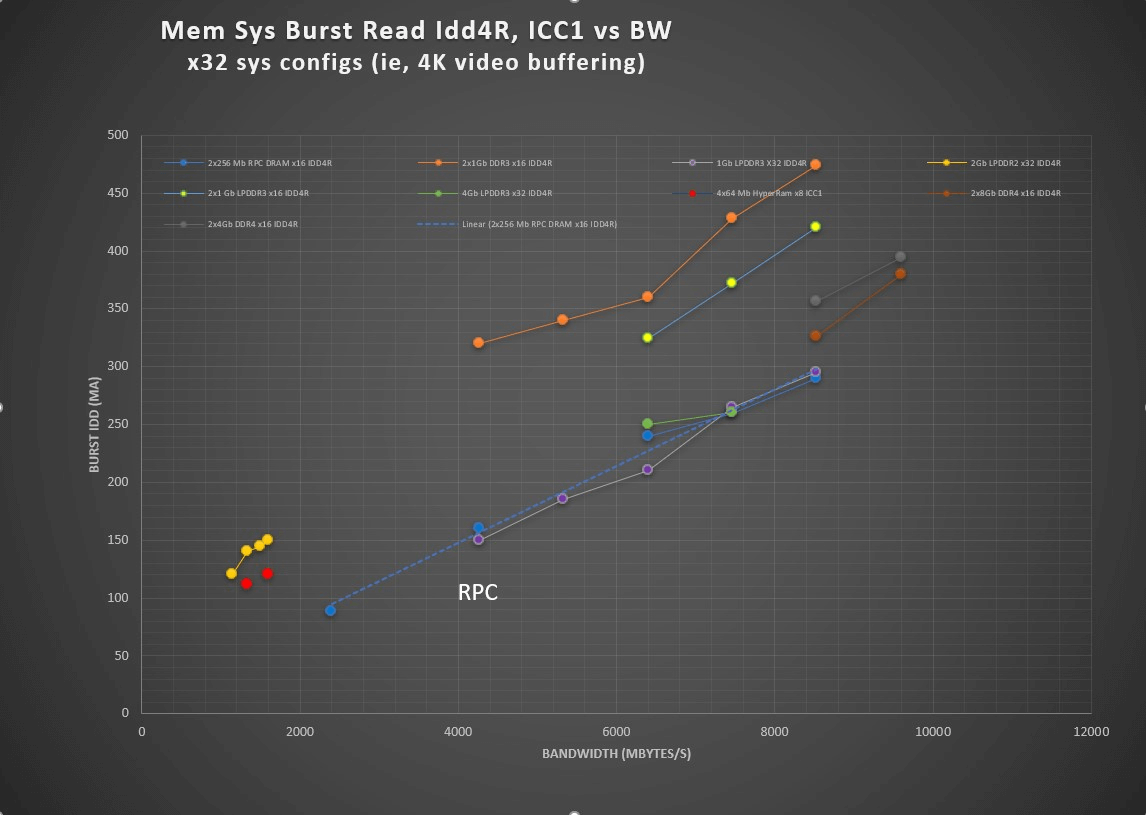
DRAM burst read current vs system bandwidth for x32 system configuration (click on the image for larger view)
The graph in Figure 7 shows the operating current for different x32-wide system configurations. These compare the total operating current for the memory ICs used in candidate physical implementations designed to meet a specific video buffer bandwidth and capacity requirement. To evaluate designs using x32 devices, the burst read operating current for a single device is plotted. For a memory system made from x16 devices, then the current for two such devices are plotted and for x8s, it is four such devices.
It is evident that no matter how these lower density buffer DRAMs are compared, the RPC offers the lowest operating current solution of the available configurations for these high-bandwidth, but low-capacity buffering applications.
As mentioned earlier, a 4K video buffer application may need only 200 megabits. Some solutions end up selecting a 4 Gigabit device because of bandwidth & availability, not because of capacity needs. There is a power, area and cost penalty associated with that choice. As shown, overprovisioning can be costly in ways other than just the cost of the memory chips.
Other power advantages:
The RPC DRAM uses no PLL or DLL circuitry on-chip. That means the RPC DRAM can accept a halted clock and can be ready for operation within five clock cycles once the clock has restarted and stabilized. This can allow the memory channel to be quickly stopped and restarted with the application’s memory demand, offering further system power savings opportunities within the SOC/ASIC/FPGA.
Physical design of systems:
The power dissipation doesn’t tell the full story. Miniaturization is of growing importance in many applications. The WLCSP used by the RPC DRAM offers a clear miniaturization advantage over all the other high bandwidth offerings, LPDDR2/3, DDR3/4. The PCB area occupied by the memory subsystem package for the hypothetical x32 system discussed above is shown in Figure 8. For x16 organized devices, two such devices are used to make the x32 bus. Likewise, for x32 devices and x8 devices a single device and four devices are used respectively.
While the HyperRAM uses the least PCB area, its limited 400 MT/s data rate is only ¼ of the RPC, DDR3/4 solutions on a per pin basis even when compared at a modest 1600 MT/s rate. Its low bandwidth and low bitcount severely limits its use for these high bandwidth buffering applications. It fails to meet the minimum bandwidth requirements for the 4K/60-16b application when used in a x32 configuration.
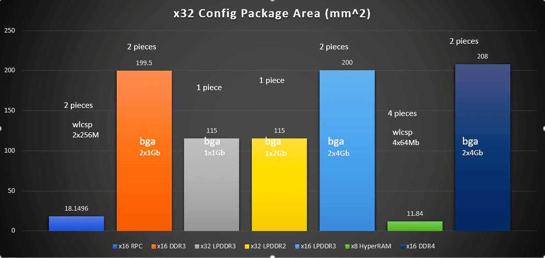
PCB area for memory packages for x32 memory subsystem (click on image for larger view).
The pincount needed to interface to the external memory subsystem is another consideration for the physical system design. The greater the pincount the more pins are needed on the SOC/ASIC/FPGA controlling the memory. More pins means there are more signals to route and that can lead to less compact PCB layouts: routing more signals can increase area and layers. Once again. the RPC DRAM is the lowest pincount among the high bandwidth choices as shown in Figure 9.
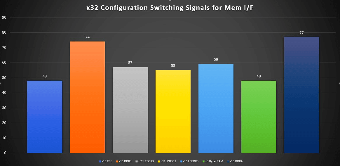
SOC/ASIC/FPGA memory interface IO pincount for x32 memory subsystem (click on image for larger view).
Manufacturing status:
The RPC DRAM is in production in the WLCSP. KGD and both BGA packages. As mentioned earlier in this document, the x16 RPC is offered in a standard 96 ball x16 DDR3 type package and bonded such that the data bus, data strobes, clocks and power pins are mapped to the same balls with all others left N/C. This has been popular for FPGA-based systems designed to use DDR3 devices. It allows a build time configuration option of using RPC or DDR3 type devices.
Conclusion:
The RPC DRAM is designed to serve the needs for high bandwidth but modest capacity memory systems such as used for video buffering and other bandwidth intensive applications. When paired with Lattice FPGAs and deployed in a distributed system architecture featuring endpoint processing, it not only avoids overprovisioning the memory system capacity, it saves power, PCB area and pincount when compared against standard DDR/LPDDR type memories. The RPC DRAM and Lattice FPGAs are available in waferscale CSP packaging, which offer the smallest and lowest cost semiconductor packages possible for a given IC. Combined with other miniaturized components, the opportunity for a new level of low-cost subsystem miniaturization using standard PCB manufacturing technology is created.
— Richard Crisp is vice president & chief scientist for imaging and memory product development at Etron Technology America