TAIPEI — In 25 years, after Facebook, Google, and Amazon have marched toward global domination by designing their own chips, what will the semiconductor industry look like? In a way, we’ve seen that future, and it’s here. Big data analysis, artificial intelligence, augmented and virtual reality, and autonomous vehicles have already emerged, although not yet in perfect form.
Nonetheless, most chip designers can’t even imagine that brave new world, let alone the inventions that they must fashion to stay relevant. A question that haunts designers is the sheer uncertainty of the industry’s direction. As Moore’s Law nears its “economic dead end” for most chip vendors (except giants like Intel and Samsung), is there somewhere else to turn?
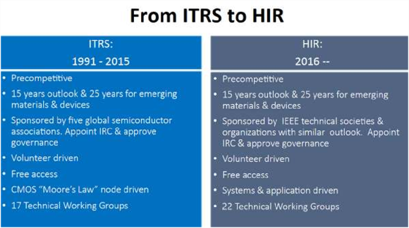
In July 2016, the Semiconductor Industry Association scrapped a technology plan widely known within the industry as the International Technology Roadmap for Semiconductors (ITRS).
SIA’s decision to end the ITRS illustrated the industry’s admission that Moore’s Law is not just slowing down. The industry needs new tools, charts, and programs to define research gaps between where it has been and where to go in an even more connected world.
This is where Nicky Lu, Chairman, CEO, and Founder of Taiwan’s Etron Technology, comes in.

Nicky Lu, CEO and Founder of Etron Technology (Photo: EE Times)
Lu has long advocated “heterogeneous integration” (HI). He promotes the idea that the semiconductor industry must, at last, outgrow its obsession with pitch shrinkage. To push growth, it must go creative with the “heterogeneous integration of different technologies.” By HI, he does not mean homogeneously integrated SoCs, Systems-in-Package (SiPs), or Multi-Chip Modules (MCMs). Lu views HI as “a holistically integrated approach” that involves system design, algorithms, and software, together with different types of silicon dice such as SoC, DRAM, flashes, A-to-D/D-to-A, power management, security, and reliability control dices.
Thus far, the chip industry has made great progress in SiP. However, Lu told us, “Now in 2018, I am seeing [the need for] even more sophisticated HI that actually integrates not only silicon dice but also non-silicon materials.”
Three IEEE societies behind HI
The groundwork to develop a Heterogeneous Integration Roadmap (HIR) began in 2015, when the SIA and one of the IEEE Societies signed an MOU, according to Bill Bottoms, chairman of Third Millennium Test Solutions (3MTS). Bottoms is a co-chair of HIR, along William Chen, ASE Fellow at ASE Group.
By 2016, HIR got official sponsorships from three IEEE Societies: the IEEE Electronics Packaging Society (EPS), IEEE Electronic Devices Society (EDS), and IEEE Photonics Society. Semiconductor Equipment and Materials International (SEMI) and the American Society of Mechanical Engineers (ASME)’ Electronic and Photonic Packaging Division (EPPD) also signed up to work on HIR.
The wheels really started to churn last year. As the HIR group held workshops throughout the world to evangelize its mission, “close to 1,000 scientists, researchers, and senior engineers showed up and pledged to participate in HIR,” said Bottoms. When it comes to its membership, “We are keeping the quality of standards very high,” he stressed. “We are picking only those with technical credentials and real commitment to contribute to each technical working group.” Typical marketing onlookers who just want to suck up information aren’t included, explained Bottoms.
Bottoms defines the scope of the HIR as “identification of the difficult challenges we need to overcome in meeting technical requirements for the next 15 years and 25 years for emerging research areas.” The group is developing a “pre-competitive” roadmap, he noted. It’s far more efficient in pooling industry resources to chart the future instead of fragmenting efforts and diverging
into too many directions. The HIR group sees the primary integration technology for potential solutions as “complex SiP architectures.”
In many ways, Bottoms said that the industry has begun to see products in which silicon dice and non-silicon materials are together in one package. “One good example of HI is Intel’s photonics optical transceivers,” he noted, in which Intel applied silicon wafer planar manufacturing technology to the volume manufacture of electro-optical transceivers.
Another example is what’s known as “S2,” the second-generation SiP in the Apple Watch 2. Just like S1, these SiP modules mix package styles in one module. The module contains components that can be packaged as bare-die (CSP, WLP, etc.) or traditional wire-bonded packages, or even multi- chip configurations like package-on-package or a multi-die memory DRAM or NAND. “Apple has pushed the SiP concept so far out into the future — a road nobody has taken before,” said Bottoms. TechInsights, in its Apple Watch 2 teardown < http://www.techinsights.com/about- techinsights/overview/blog/apple-watch-series-2-teardown/> , wrote, “The S2 contains more than 42 die! That is a lot of silicon in such a small module.” Similarly, Bottoms was marveled at the 98 interconnects inside S2.
Nothing pleases Lu more than the growing momentum behind HI. Heterogeneous integration is no longer just his passion, but is spreading throughout electronics, Lu told us.
Earlier this year, Lu gave a plenary talk entitled “Synergistic Growth of AI and Silicon Age 4.0 through Heterogeneous Integration of Technologies” at an IEEE-organized event < http://www.cpmt.org/scv/?p=513> in Santa Clara. He told us, “So many people came to see me after my speech. They were all so excited.”
What’s so exciting? Lu’s talk wasn’t about the nuts and bolts of integrating heterogeneously. Instead, he described his focus as broadening the scope of research and development in the semiconductor industry.
Now that the chip industry is no longer hostage to continuous scaling, Lu believes that it can apply its knowledge to a larger mission. The next step, he says, is “pervasive intelligence” enabled across different industries ranging from AI, human, and natural interface to bio, cells, bacteria, and medical intelligence.
It’s one thing to discuss best designs for next-generation AI chips. Everyone does. But if the industry wants a “roadmap” to extend forward 25 years, it’d better start making intelligence pervasive, explained Lu.
Obsession
Before describing what Lu defines as “pervasive intelligence,” it’s important to understand how Lu’s interest in heterogeneous integration has evolved.
Born and educated in Taiwan, Lu earned his M.S. and Ph.D. in Electrical Engineering from Stanford University. At the IBM Research Div., where he started his career, he’s known as a co-inventor of a 3D-DRAM technology and a designer of High-Speed CMOS DRAM (HSDRAM).
Over several decades, this technical virtuosity, abetted by an infectious smile and passionate demeanor, have made Lu a vocal force within the semiconductor industry.
Lu has advocated Heterogeneous Integration ever since delivering a plenary talk at the 2004 International Solid-State Circuits Conference (ISSCC). He pointed out that “future system chips will fully utilize multi-dimensional integration, within a single package, of multiple dies that cover a variety of digital, analog, memory, and RF functions and technologies.”
Lu’s prediction of an emerging era of 3D ICs was considered bold then. He wanted to demonstrate what could be accomplished by the vertical integration of dice at a time when the chip world was largely content to follow Moore’s Law — whose sole precept is the constant scaling of transistors.
Advancement in packaging
Fast forward to 2018, when it’s fair to argue that the era of the SiP is already here and the death of Moore’s Law is greatly exaggerated.
The packaging technology that the chip industry knew in 2004 has made remarkable strides. Consider the integrated fan-out (InFO) wafer-level packaging technology achieved by the Taiwan Semiconductor Manufacturing Co. TSMC’s InFO enabled Apple to offer a very thin package-on- package, with a high number of I/O pads and better thermal management for the A10 applications processor in the iPhone 7.
The InFO platform’s re-distributed layer technology connects silicon dice directly to the PCB level without another substrate layer. TSMC-designed Through Interconnect Via (TIV) “can provide pillars to connect different dice or components using mixed vertical and horizontal interconnect technologies,” noted Lu. InFO demonstrated a link between its short vertical and long horizontal connections, speeding information travel.
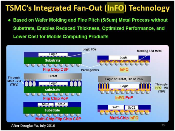
TSMC’s InFO Technology
Lu is hopeful for the future of heterogeneous integration technologies. TSMC’s 3D wafer-based system integration — including chip-on-wafer-on-substrate and integrated fan-out, is a great example, he said, because it shows how to achieve another level of micro-system performance and stacking.
It was Apple, not a traditional chip vendor, who pushed TSMC toward the InFO breakthrough. Examples of what Apple has done with A10 or its second-generation SiP for Apple Watch 2 illustrate, in Lu’s opinion, that the chip industry must look beyond itself. It must unearth “intelligent” solutions hotly pursued not just by fellow chip vendors but other industries.
Lu believes that the heterogeneous integration roadmap will push not just chipmakers but “many industries searching for new applications to add more values with IC-centric system solutions.”
Using protein as hardware, DNA as software
Lu’s plenary talk at the HIR meeting in February was inspiring to many because Lu was stretching
the concept of HI into the future. He cited cell intelligence as an example of where the electronics industry’s expertise can be leveraged.
“Think about using protein as a piece of hardware and DNA as software that runs on top of it,” said Lu. He was referring to what is known as synthetic biological circuits. Biological parts inside a cell are designed to perform logical functions mimicking those observed in electronics circuits.
Lu apologized for boasting the cell therapy research pursued by his son, Timothy Lu, but noted that building new gene circuits is no longer a pipe dream. Lu’s son, an associate professor of Biological Engineering, Electrical Engineering, and Computer Science at MIT, is a founder of Senti Bio, a synthetic biology startup that raised $53 million in series A funding earlier this year.
Timothy Lu described his startup, in a recent interview with Symbiobeta, as a company “focused on using synthetic biology tools to build next-generation cell and gene therapies that can adapt, sense, respond, and have a greater range of effects than current cell and gene therapies are capable of.”
Discussing plans to bring in best-of-class technologies from different labs, he said, “Collectively, these labs have shown that you can program sophisticated logic with multi-input, multi-output (MIMO) types of systems.”
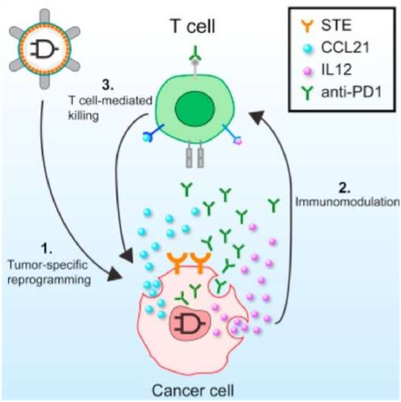
Synthetic RNA-Based Immunomodulatory Gene Circuits for Cancer Immunotherapy (Source: www.cell.com)
Other ubiquitous intelligence examples include a pill — a small optical device made through heterogeneous integration. After the patient swallows it, the pill functions as a tiny computer collecting data and offering intelligence, said Lu. Think “Fantastic Voyage” but without Raquel Welch.
Life intelligence is another area where intelligence can be embedded into materials. AI can be built into materials, said Lu, to monitor their “health.”
But wait. There’s more. “Microbiome,” he said, is the collection of microorganisms that live in people. Quoting his son’s research again and profusely apologizing for doing so, Lu explained that therapeutics targeting the human microbiome are rapidly developing.
A book entitled “Engineering the Microbiome for Human Health Applications,” co-authored by Timothy Lu and others, indicates that microbiome therapeutics could construct “clinically relevant biosensors, engineering robust and effective synthetic gene circuits that can function in vivo.”
As interesting as it was to ponder bio-science, we had to stop Lu and ask: What tangible benefits could the semiconductor industry deliver to such R&D projects in the world of “pervasive intelligence”?
Lu said, “The knowledge, expertise, and theories we learned in computing are essential, and they are transferable to other fields.” Lu rhetorically asked: “What did silicon technology teach us?” It taught us how to make things smaller and calculate data much faster, he said. The mystery of scaling solved by the chip industry can now apply to creating nano-modules for artificial intelligence, IoT, and living things.
Lu is banking on the industry to produce application-driven HI nano-systems. “We can accomplish this by optimizing physics, materials, devices, circuits/chips, software, and systems.”
Unveiling of HI roadmap
The HIR group plans to unveil fruits of their work at SEMICON West. Each of 22 HIR technical working groups is writing a chapter of the roadmap to be peer-reviewed, edited, finalized, and presented at the conference. The technical documents will be available to the public in July. The group is preparing to post an online version “shortly after SEMICON West,” according to Bottoms.
The 22 chapters covered in the HI roadmap include everything from “HI for Market Application,” “Heterogeneous Integration Components,” and “Design (Co-Design and Simulation, Tools & Practice)” to “cross-cutting topics” such as materials and “interconnect and integration processes” such as SiP, 3D + 2.5D, and WLP (fan-in and fan-out).
Bottoms noted that “thermal management” and “security” were two late additions. HIR participants identified them as crucial, he said. Their findings “serve the technical working groups across the board.” Noting that the thermal management group is led by a guy from Google, Bottoms emphasized that HIR has support from the leading companies in the industry. “Many senior people from Intel, Google, and IBM are active members.”
In addition to HIR, there are two other industry groups pushing post-ITRS roadmaps. One is the International Technology Roadmap for Devices and Systems (IRDS) sponsored by the IEEE Standards Association and associated with the Rebooting Computing Initiative. Another is the International Technology Roadmap for Wide Band-Gap Semiconductors (ITRW) sponsored by the IEEE Power Electronics Society.
None claim that it’s better than the others. Instead, stressed Bottoms, “these roadmaps look at the future from the three vantage points of their technology space. Together, they complement each other in their harmonized complexity providing multi-dimension vision for the future for the electronic industry.”
(Source: Heterogeneous Integration Roadmap Working Group)
All this churn begs the question, however, of why the electronics industry loves to draw “roadmaps.” Has everyone been brainwashed by Moore’s Law?Indeed, Moore’s Law got everyone in the industry dancing to a common tune, keeping its products and R&D plans in step.
Bottoms believes that having the roadmap will be even more vital in fulfilling the potential of Heterogeneous Integration. It can guide “the professions, industries, academia, and government to identify key technical challenges with sufficient lead time that they do not become roadblocks preventing the continued progress in electronics and their widespread application and implementation into diverse industries,” he wrote in the technical paper entitled “Heterogeneous Integration Roadmap < https://ieeexplore.ieee.org/document/7939380/> ,” co-authored with Chen.
Chen and Bottoms concluded that “the goal is to stimulate research and innovations and collaboration across the entire ecosystem so that progress may continue unimpeded in achieving the future vision.”
Source: https://www.eetimes.com/chip-industry-maps-heterogeneous-integration/