歡迎參觀鈺創科技於 #COMPUTEX2026 與USB Community的展位,一同探索「AI TOGETHER」新世代邊緣智慧應用!
誠摯邀請您蒞臨參觀,與鈺創科技共同探索 AI 生態系的未來藍圖!
📍 鈺創科技集團攤位:南港展覽1館4樓 L0401a
📍 USB Community:南港展覽1館4樓 N0614
📅 展覽日期:2026/06/02 – 06/05
The Abu Dhabi AI Summit-Symbiotic Growth between Semiconductor and AI Industries for Booming IntelligenceN Economy
-
Symbiotic Growth of AI and Semiconductors: The presentation emphasizes the mutual reinforcement between AI and semiconductor industries, driving a booming “IntelligenceN” economy through innovations in Silicon 4.0 and Heterogeneous Integration (HI).
-
Evolution of Moore’s Law and OMHI: It introduces a “2nd Path” for Moore’s Law, focusing on Optimized Monolithic & Heterogeneous Integration (OMHI) to overcome physical scaling limits and address memory wall and energy challenges.
-
Emergence of Self-Smart Microsystems: The future points toward “Self-Smart Microsystems” that integrate logic, memory (DRAM), and AI hardware/software to enable diverse applications ranging from edge AI to bio-medical logic gates.

“MemorAiLink® Show Up” at CES 2026:Etron Tech Advances Edge AI and Robotics through On-Device Innovation
- RPC® inside G120 Subsystem – Honored with the “2025 Hsinchu Science Park Innovative Product Award.”
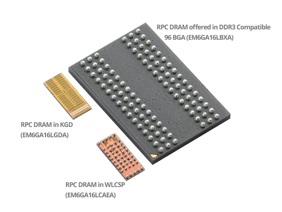
- New Scalable DDR3 Products and ASIC AI Memory – Developed through the MemorAiLink®
- EJ732 Series Chips – Successfully obtained the USB-IF USB PD3.2 DRP Controller Certification.
- Launch of Robotics Barebone Platforms – Introducing the AMR01C and AMR01M
- XINK Nano Platform –Successfully deployed in smart parking applications by Taiwan’s leading EV charging system integrator.
- Strategic Partnership with Asia Optical – Collaborating to create domestic delivery and robotic base barebone systems.
- Privacy-First AI Robot Decision System – Winner of the CES Innovation Award.
- “DecloakVision” – Recognized with the 22nd National Innovation Award.

【會員專屬 登入查閱全文】
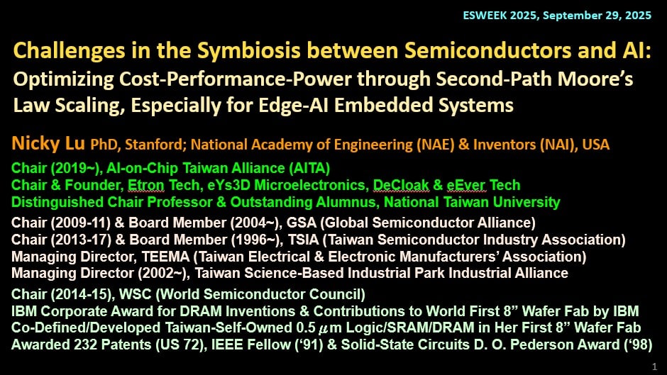
ESWEEK 2025 – Embedded System Week – Dr Nicky Lu’s Slide Deck
Challenges in the Symbiosis between Semiconductors and AI: Optimizing Cost-Performance-Power through Second-Path Moore’s Law Scaling, Especially for Edge-AI Embedded Systems
【會員專屬 登入查閱全文】
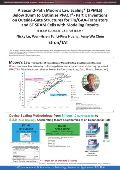
A Second-Path Moore’s Law Scaling (2PMLS) Below 10nm to Optimize PPACT- Part I: Inventions on Outside-Gate Structures for Fin/GAA-Transistors and 6T SRAM Cells with Modeling Results
《A Second-Path Moore’s Law Scaling (2PMLS) Below 10nm to Optimize PPACT – Part I》。本篇聚焦於10奈米以下節點的創新途徑,深入探討FinFET與GAA晶體管結構的外閘技術(Outside-Gate Structures),以及6T SRAM單元的設計優化。
【會員專屬 登入查閱全文】
Challenges to Symbiotic Growth of Semiconductor & AI Industries: A 2nd-Path Moore’s Law Scaling for Deep, Broad, and Exponential Intelligence Economics
DRC是一個透過動手設計、團隊合作與問題解決來促進創新的平台。它鼓勵跨部門協作與實作學習,推動具實質價值的研發成果。
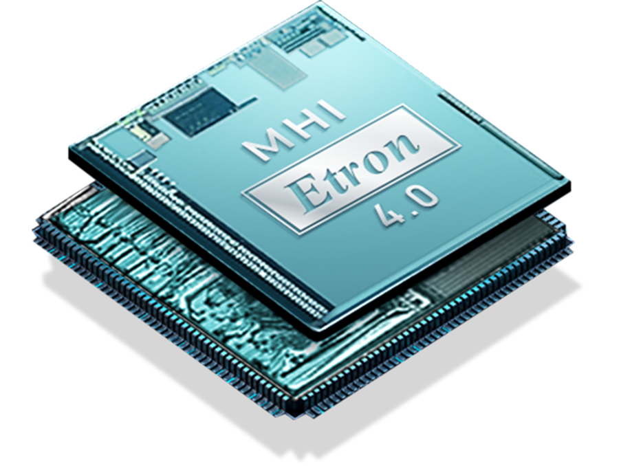
同體異質整合加乘 (Monolithic and Heterogeneous Integration, MHI™)
- 將矽和非矽之材料與元件的同體異質整合最佳化
- 創造由奈米矽核心與AI技術支援的Self-Smart微系統